ОПИСАНИЕ
LT3905 - это повышающий преобразователь с фиксированной частотой в режиме тока, предназначенный для смещения лавинных фотодиодов (APD) в оптических приемниках. LT3905 обеспечивает контроль тока APD на высокой стороне в четырех декадах динамического диапазона с относительной точностью более 2% в диапазоне от 3 мкА до 3 мА.
Максимальный ток APD программируется с помощью одного резистора, а быстрый ограничитель тока с индикатором защищает APD в условиях перегрузки. Регулируемое выходное напряжение обеспечивает динамическое управление смещением, а регулируемый индикатор потери сигнала сигнализирует о низком токе APD.
В сочетании со встроенным DMOS-переключателем питания и выпрямителем Шоттки LT3905 представляет собой компактное комплексное решение с небольшим количеством внешних компонентов и низкой стоимостью. Постоянная частота переключения приводит к предсказуемым выходным шумам, которые легко фильтровать.
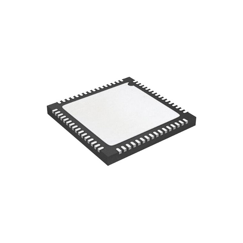
LT3905 выпускается в миниатюрном (3 мм × 3 мм) 16-выводном корпусе QFN.
ОСОБЕННОСТИ
65 В, 350 мА Внутренний переключатель DMOS
Интегрированный диод Шоттки
2% Точный мониторинг тока APD в диапазоне от 3 мкА до 3 мА
Программы с одним резистором Максимальный ток APD
Быстрый ограничитель тока APD с индикатором
Программируемый индикатор потери сигнала
Вывод CTRL регулирует выходное напряжение
Программируемая блокировка пониженного напряжения VIN
Высокоэффективный повышающий преобразователь
Выбираемая частота переключения 1МГц/2МГц
Внутреннее вознаграждение
Внутренний плавный пуск
Диапазон VIN от 2,7 В до 12 В
Низкий ток выключения: <1 мкА
ПРИЛОЖЕНИЯ
Предвзятое отношение к APD
Подводка PIN-диода
Оптические приемники и модули
Оборудование для оптоволоконных сетей
ОПЕРАЦИЯ
Обзор
LT3905 объединяет 65-вольтовый повышающий DC/DC-преобразователь с токовым режимом и комбинированный APD-монитор и регулятор тока, обеспечивая точный контроль и эффективное питание, а также дополнительную гибкость и защиту.
Повышающий преобразователь использует 65 В, 0,75 Ом DMOS-переключатель питания и встроенный диод Шоттки для преобразования низкого входного напряжения в более высокое напряжение, подходящее для питания APD. Повышающий преобразователь работает на фиксированной частоте, в токовом режиме с внутренней компенсацией и точным ограничением тока.
ИНФОРМАЦИЯ О ПРИЛОЖЕНИЯХ
Частота переключения
LT3905 позволяет выбирать частоту переключения между 1 и 2 МГц. Подключите вывод fSEL к напряжению более 0,9 В, чтобы выбрать режим 2 МГц, или подключите к GND, чтобы выбрать режим 1 МГц.
Обратная связь по напряжению
Усилитель ошибки LT3905 оснащен как фиксированным внутренним опорным напряжением 1,248 В, так и регулируемым входом внешнего опорного напряжения (CTRL). Эта функция позволяет пользователям выбирать между использованием встроенного опорного напряжения и внешнего опорного напряжения при программировании выходного напряжения. Можно регулировать напряжение на выводе CTRL во время работы устройства, чтобы изменять выходное напряжение LT3905 и, следовательно, напряжение смещения APD.
Выбор индуктора
Индуктивность, используемая с LT3905, должна иметь номинал насыщения 400 мА или выше. Если устройство используется в приложении, где входной источник питания подключается в горячем режиме, ток насыщения должен превышать пиковый пусковой ток.
Монитор тока APD Переходный отклик
Переходный отклик монитора тока APD является ключевой характеристикой. Она в основном зависит от уровня сигнала, поскольку полоса пропускания малого сигнала увеличивается с ростом входного сигнала.
При токе более 10 мкА токовое зеркало APD LT3905 обычно имеет время отклика в несколько сотен наносекунд. Для измерения такого быстрого переходного отклика используется широкополосный трансимпедансный усилитель на LT6210, как показано на рисунке 6. Работая в шунтирующей конфигурации, усилитель буферизирует выход MON и значительно снижает эффективный выходной импеданс. Обратите внимание, что в итоговом измерении присутствует инверсия и смещение опорного постоянного тока.
Подсказки по расположению
Высокая скорость работы LT3905 требует внимательного отношения к разводке платы. При небрежной разводке вы не получите заявленных характеристик. Для предотвращения проблем с излучением и высокочастотным резонансом очень важно правильно расположить высокочастотный коммутационный тракт. Располагайте выходной конденсатор как можно ближе к диоду Шоттки (вывод VOUT). Минимизируйте длину и площадь всех трасс, подключенных к выводу переключателя, и всегда используйте плоскость заземления под переключающим регулятором, чтобы минимизировать межплоскостную связь. Путь сигнала, включающий переключатель, выходной диод и выходной конденсатор, имеет наносекундное время нарастания и спада и должен быть как можно короче.