ОПИСАНИЕ
The LT8645S/LT8646S synchronous step-down regulator features second generation Silent Switcher architecture designed to minimize EMI emissions while delivering high efficiency at high switching frequencies. This includes the integration of bypass capacitors to optimize all the fast current loops inside and make it easy to achieve advertised EMI performance by eliminating layout sensitivity.
The fast, clean, low-overshoot switching edges enable high efficiency operation even at high switching frequencies, leading to a small overall solution size. Peak current mode control with a 40ns minimum on-time allows high step-down ratios even at high switching frequencies. The LT8646S has external compensation to enable current sharing and fast transient response at high switching frequencies.
Режим Burst Mode обеспечивает сверхнизкое потребление тока в режиме ожидания, режим пропусков импульсов - полную частоту переключения при более низких выходных нагрузках, а режим разнесенного спектра позволяет дополнительно снизить уровень электромагнитных помех.
ОСОБЕННОСТИ
Архитектура бесшумного коммутатора
Сверхнизкое электромагнитное излучение на любой печатной плате
Устранение чувствительности макета печатной платы
Внутренние шунтирующие конденсаторы снижают уровень излучаемых электромагнитных помех
Дополнительная модуляция с использованием разнесенного спектра
Высокая эффективность при высокой частоте
Эффективность до 95% на частоте 1 МГц, от 12 ВИН до 5 ВЫХ
Эффективность до 94% на частоте 2 МГц, от 12ВИН до 5ВЫХ
Широкий диапазон входного напряжения: 3,4 В - 65 В
Сверхнизкий ток покоя Режим серийной работы
2.5μA IQ Regulating 12VIN to 3.3VOUT (LT8645S)
Колебания выходного сигнала < 10 мВП-П
External Compensation: Fast Transient Response and Current Sharing (LT8646S)
Быстрое минимальное время включения: 40 нс
Низкое падение напряжения при любых условиях: 60 мВ при 1 А
Регулируемый и синхронизируемый: от 200 кГц до 2,2 МГц
Работа в режиме пикового тока
Плавный пуск и отслеживание выходного сигнала
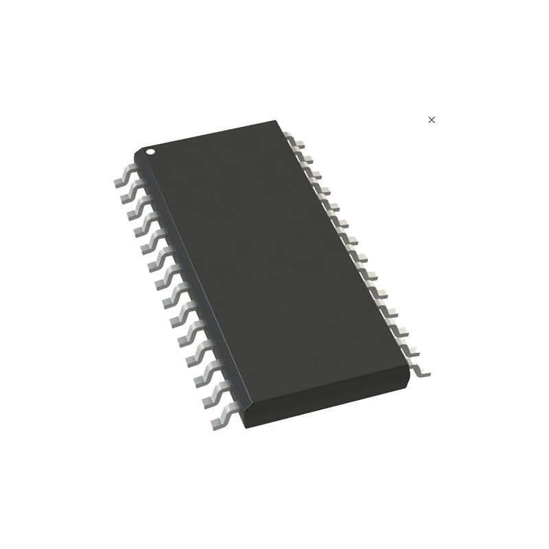
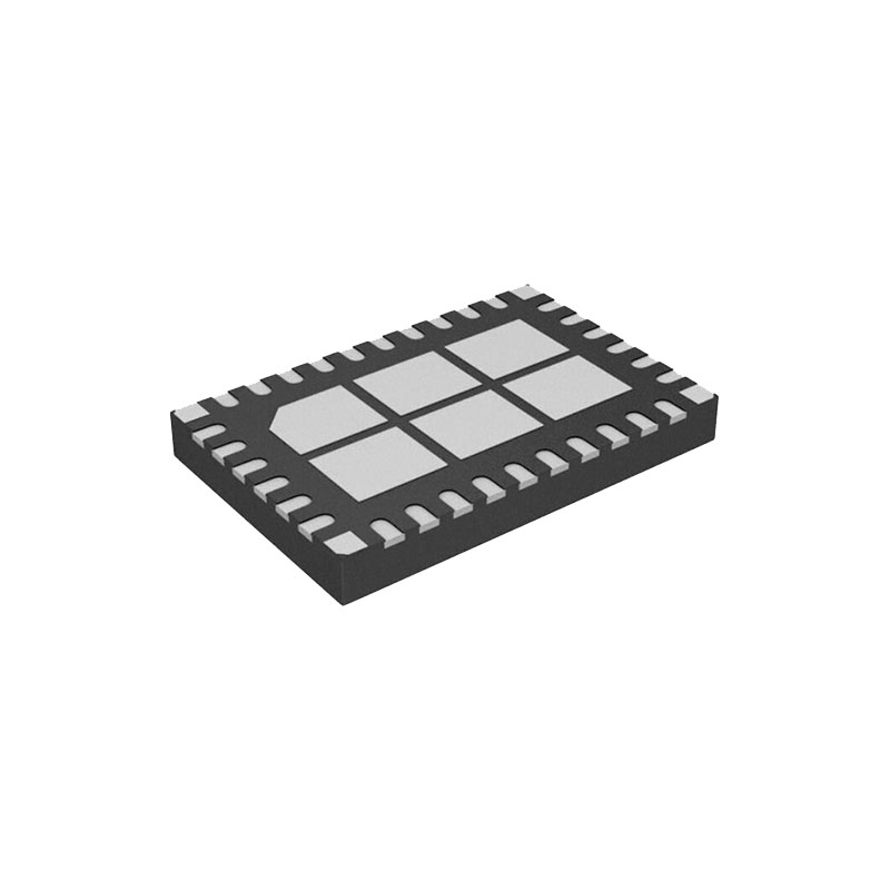
Малогабаритный 32-выводной корпус LQFN размером 6 мм × 4 мм
Квалификация AEC-Q100 для применения в автомобильной промышленности
ПРИЛОЖЕНИЯ
Автомобильные и промышленные принадлежности
Понижающий генератор общего назначения
Источники питания GSM
ОПЕРАЦИЯ
The LT8645S/LT8646S is a monolithic, constant frequency, current mode step-down DC/DC converter. An oscillator, with frequency set using a resistor on the RT pin, turns on the internal top power switch at the beginning of each clock cycle. Current in the inductor then increases until the top switch current comparator trips and turns off the top power switch. The peak inductor current at which the top switch turns off is controlled by the voltage on the internal VC node. The error amplifier servos the VC node by comparing the voltage on the VFB pin with an internal 0.97V reference. When the load current increases it causes a reduction in the feedback voltage relative to the reference leading the error amplifier to raise the VC voltage until the average inductor current matches the new load current. When the top power switch turns off, the synchronous power switch turns on until the next clock cycle begins or inductor current falls to zero. If overload conditions result in more than 11A flowing through the bottom switch, the next clock cycle will be delayed until switch current returns to a safe level.
The “S” in LT8645S/LT8646S refers to the second generation Silent Switcher technology. This technology allows fast switching edges for high efficiency at high switching frequencies, while simultaneously achieving good EMI performance. This includes the integration of ceramic capacitors into the package for VIN, BST, and INTVCC. These caps keep all the fast AC current loops small, which improves EMI performance.
If the EN/UV pin is low, the LT8645S/LT8646S is shut down and draws approximately 1μA from the input. When the EN/UV pin is above 1.01V, the switching regulator will become active.
To optimize efficiency at light loads, the LT8645S/LT8646S operates in Burst Mode operation in light load situations. Between bursts, all circuitry associated with controlling the output switch is shut down, reducing the input supply current to 1.7μA (LT8645S) or 230μA (LT8646S with BIAS = 0). In a typical application, 2.5μA (LT8645S) or 120μA (LT8646S with BIAS = 5VOUT) will be consumed from the input supply when regulating with no load. The SYNC/MODE pin is tied low to use Burst Mode operation and can be floated to use pulse-skipping mode. If a clock is applied to the SYNC/MODE pin, the part will synchronize to an external clock frequency and operate in pulse-skipping mode. While in pulse-skipping mode the oscillator operates continuously and positive SW transitions are aligned to the clock. During light loads, switch pulses are skipped to regulate the output and the quiescent current will be several hundred μA.
To improve EMI, the LT8645S/LT8646S can operate in spread spectrum mode. This feature varies the clock with a triangular frequency modulation of +20%. For example, if the LT8645S/LT8646S’s frequency is programmed to switch at 2MHz, spread spectrum mode will modulate the oscillator between 2MHz and 2.4MHz. The SYNC/MODE pin should be tied high to INTVCC (~3.4V) or an external supply of 3V to 4V to enable spread spectrum modulation with pulse-skipping mode.
To improve efficiency across all loads, supply current to internal circuitry can be sourced from the BIAS pin when biased at 3.3V or above. Else, the internal circuitry will draw current from VIN. The BIAS pin should be connected to VOUT if the LT8645S/LT8646S output is programmed at 3.3V to 25V.
The VC pin optimizes the loop compensation of the switching regulator based on the programmed switching frequency, allowing for a fast transient response. The VC pin also enables current sharing and a CLKOUT pin enables synchronizing other regulators to the LT8646S.
Компараторы, контролирующие напряжение на выводе FB, подадут низкий уровень на вывод PG, если выходное напряжение будет отличаться от заданного значения более чем на ±8% (типично), или если возникнет состояние неисправности.
The oscillator reduces the LT8645S/LT8646S’s operating frequency when the voltage at the FB pin is low. This frequency foldback helps to control the inductor current when the output voltage is lower than the programmed value which occurs during start-up or overcurrent conditions. When a clock is applied to the SYNC/MODE pin, the SYNC/MODE pin is floated, or held DC high, the frequency foldback is disabled and the switching frequency will slow down only during overcurrent conditions.