Описание
The LTC5567 is optimized for RF downconverting mixer applications that require wide IF bandwidth. The part is also a pin-compatible upgrade to the LT5557 active mixer, offering higher linearity and 1dB compression, wider bandwidth, and lower output spurious levels. Integrated RF and LO transformers and LO buffer amplifiers allow a very compact solution.
The RF input is 50Ω matched from 1.4GHz to 3GHz, and easily matched for higher or lower RF frequencies with simple external matching. The LO input is 50Ω matched from 1GHz to 4GHz, even when the IC is disabled. The LO input is easily matched for higher or lower frequencies, as low as 300MHz, with simple external matching. The low capacitance differential IF output is usable up to 2.5GHz.
Характеристики
High IIP3: +26.9dBm at 1950MHz
1.9dB Conversion Gain
Low Noise Figure: 11.8dB at 1950MHz
16.5dB NF Under 5dBm Blocking
Low Power: 294mW
Wide IF Frequency Range Up to 2.5GHz
LO Input 50Ω Matched when Shutdown
–40°C to 105°C Operation (TC)
Very Small Solution Size
Pin Compatible with LT5557
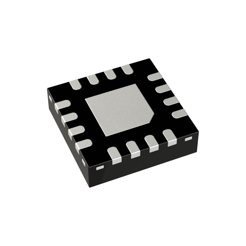
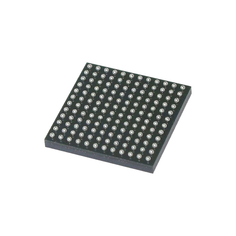
16-Lead (4mm × 4mm) QFN package
Приложения
Wireless Infrastructure Receivers
DPD Observation Receivers
CATV Infrastructure
ИНФОРМАЦИЯ О ПРИЛОЖЕНИЯХ
Введение
The LTC5567 incorporates a high linearity double-balanced active mixer, a high-speed limiting LO buffer and bias/enable circuits. See the Pin Functions and Block Diagram sections for a description of each pin. A test circuit schematic showing all external components required for the
data sheet specified performance. A few additional components may be used to modify the DC supply current or frequency response, which will be discussed in the following sections.
The LO and RF inputs are single ended. The IF output is differential. Low side or high side LO injection may be used. The test circuit,utilizes bandpass IF output matching and an 8:1 IF transformer to realize a 50Ω single-ended IF output.
Вход LO
A simplified schematic of the LO input. Similar to the RF input, the integrated LO transformer’s primary winding is DC-grounded internally, and therefore requires an external DC-blocking capacitor. Capacitor C5 provides the necessary DC-blocking, and optimizes the LO input match over the 1GHz to 4GHz frequency range. The nominal LO input level is 0dBm although the limiting amplifiers will deliver excellent performance over a ±5dB input power range. LO input power greater than +6dBm may cause conduction of the internal ESD diodes.
The IF matching uses 249Ω resistors and 390nH supply chokes to produce a wideband 200Ω differential output. This differential output is suitable for driving a wideband differential amplifier, filter, or a wideband 4:1 transformer. The evaluation board layout allows the removal of the IF transformer to evaluate the mixer performance with a differential output.
The complete test circuit, uses resistive impedance matching attenuators (L-pads) on the evaluation board to transform each 100Ω IF output to 50Ω. An external 0°/180° power combiner is then used to convert the 100Ω differential output to 50Ω single-ended, to facilitate measurement.
Highpass IF Matching
By simply changing component values, the bandpass IF output matching network can be changed to a highpass impedance transforming network. This matching network will drive a lower impedance differential load (or transformer), like the 200Ω wideband bandpass matching previously described, while delivering higher conversion gain, similar to the 400Ω bandpass matching. The highpass matching network will have less IF bandwidth than the bandpass matching. It also uses smaller inductance values; an advantage when designing for IF center frequencies well below 100MHz.
Supply Voltage Ramping
Fast ramping of the supply voltage can cause a current glitch in the internal ESD clamp circuits connected to the VCC pin. Depending on the supply inductance, this could result in a supply voltage transient that exceeds the 4.0V maximum rating. A supply voltage ramp time greater than 1ms is recommended.

