ОБЩЕЕ ОПИСАНИЕ
LTC5596 - это высокоточный среднеквадратичный детектор мощности, обеспечивающий очень широкую полосу пропускания радиочастотного сигнала - от 100 МГц до 40 ГГц. Это делает устройство подходящим для широкого спектра ВЧ и СВЧ приложений, таких как микроволновые линии связи "точка-точка", приборы и приложения управления мощностью. Выходное напряжение постоянного тока детектора является точным отображением средней мощности сигнала, подаваемого на ВЧ-вход. Отклик линейный по дБ с логарифмическим наклоном 29 мВ/дБ в динамическом диапазоне 35 дБ с точностью, как правило, лучше ±1 дБ. Детектор особенно хорошо подходит для измерения форм сигнала с коэффициентом гребня (CF) до 12 дБ, а также форм сигнала, которые демонстрируют значительное изменение коэффициента гребня во время измерения. Для достижения более высокой точности и снижения пульсаций на выходе полоса усреднения может быть отрегулирована извне с помощью конденсатора, подключенного между выводами FLTR и OUT. Интерфейс разрешения переключает устройство между активным режимом измерения и режимом отключения с низким энергопотреблением.
ОСОБЕННОСТИ
Сверхширокий диапазон согласованных входных частот: 100 МГц - 40 ГГц
Линейный динамический диапазон 35 дБ (ошибка < ±1 дБ)
29 мВ/дБ Логарифмический наклон
Плоская характеристика ±1 дБ в диапазоне от 200 МГц до 30 ГГц
Точное измерение среднеквадратичной мощности модулированных сигналов с высоким коэффициентом гребенки (до 12 дБ)
Режим отключения при низком энергопотреблении
Низкий ток питания: 30 мА при 3,3 В (типичный)
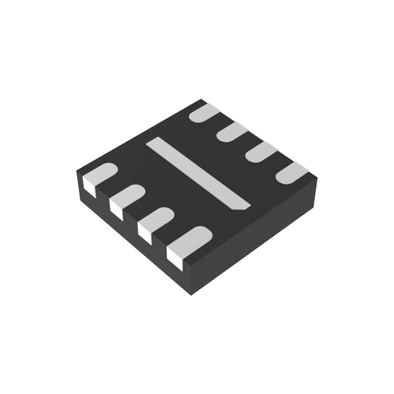
Маленький пластиковый корпус DFN8 размером 2 мм × 2 мм
I класс: от -40°C до 105°C Номинальный H класс: от -40°C до 125°C Номинальный с гарантированным логарифмическим уклоном и логарифмическим интерцептом
Рейтинг ESD: 3500V HBM, 1500V CDM
ПРИЛОЖЕНИЯ
Микроволновые линии связи "точка-точка
Приборы и измерительное оборудование
Военные радиостанции
Беспроводные сети LTE, WiFi, WiMax
Измерение среднеквадратичной мощности
Управление коэффициентом усиления при приеме и передаче
Управление мощностью передачи RF PA
ИНФОРМАЦИЯ О ПРИЛОЖЕНИЯХ
LTC5596 - это истинный среднеквадратичный детектор мощности радиочастотного сигнала, способный измерять радиочастотный сигнал в диапазоне частот от 100 МГц до 40 ГГц, независимо от входных форм сигналов с различными коэффициентами гребня, таких как сигналы CW, WCDMA, OFDM (LTE и WiFi). Динамический диапазон до 35 дБ достигается с очень стабильным выходом во всем диапазоне температур корпуса.
Радиочастотный вход
Односторонний ВЧ-вход имеет внутреннее согласование 50 Ом как в активном режиме, так и в режиме отключения с низким энергопотреблением. Во избежание повреждения внутренней схемы постоянное напряжение, подаваемое на этот вывод, должно быть ниже 1 В. Вместе с выводами 5 и 7 GND, RFIN (вывод 6) образует
Чтобы минимизировать отражения на высоких частотах, центральная полоса была выбрана такой же ширины, как и контакт RFIN (10 мил). Аналогично, центральный контакт 2,92-миллиметрового разъема 40 ГГц, оконечного с другой стороны GCPW, также имеет ширину 10 мил. На оценочной плате LTC5596 в качестве верхней подложки используется слой материала Rogers RO3003 толщиной 5 мил для достижения низких диэлектрических потерь до 40 ГГц. Две другие подложки на плате представляют собой обычный материал FR-4. При такой конфигурации характеристический импеданс 50 Ом достигается при ширине зазора 9 мил между центральной полосой и двумя проводниками возврата на землю. Виа, соединяющие верхние проводники заземления со второй металлической плоскостью заземления, должны быть размещены вдоль края верхних проводников заземления GCPW. Размеры виа должны быть как можно меньше; на оценочной плате используются виа диаметром 6 мил; 8 мил с учетом металлического краевого кольца (пончика).
Интерфейс FLTR (вывод 3):
Этот вывод позволяет дополнительно подавить высокочастотные пульсации выходного сигнала детектора за счет более медленного отклика детектора (большее время нарастания, спада и задержки распространения). Внешний конденсатор C3, подключенный между FLTR и OUT, увеличивает емкость обратной связи через выходной усилитель и уменьшает полосу пропускания выходного фильтра, не влияя на возможности LTC5596 по управлению током. Подходящие значения емкости находятся в диапазоне от 10пФ до 1нФ, но суммарная емкость обратной связи и нагрузки (от OUT до сигнальной земли) не должна превышать 1нФ. Большие значения емкости могут привести к нестабильной работе выходного драйвера.
Чтобы избежать необратимого повреждения микросхемы, постоянное напряжение на выводе FLTR не должно превышать 0,4 В. Также не рекомендуется подавать на этот вывод постоянный ток смещения, превышающий примерно 100 мкА.