ОПИСАНИЕ
The M24C01(C02) is a 1(2)-Kbit I2C-compatible EEPROM (electrically erasable programmable memory) organized as 128 (256) × 8 bits.
The M24C01/02-W can be accessed with a supply voltage from 2.5 V to 5.5 V, the M24C01/02-R can be accessed with a supply voltage from 1.8 V to 5.5 V, and the M24C02-F can be accessed either with a supply voltage from 1.7 V to 5.5 V (over the full temperature range) or with an extended supply voltage from 1.6 V to 5.5 V under some restricted conditions. These devices operate with a maximum clock frequency of 400 kHz.
ОСОБЕННОСТИ
I²C interface
• Compatible with following I²C bus modes:
– 400 kHz (Fast mode)
– 100 kHz (Standard mode)
Memory
• 1-Kbit (128-byte) of EEPROM
• 2-Kbit (256-byte) of EEPROM
• Page size: 16-byte
Supply voltage
• Wide voltage range: From 1.6 V to 5.5 V
– M24C01/02-W: 2.5 V to 5.5 V
– M24C01/02-R: 1.8 V to 5.5 V
– M24C02-F:1.7 V to 5.5 V , 1.6 V to 5.5 V (under temperature constraint)
Temperature
• Operating temperature range: from -40 °C up to +85 °C
Fast write cycle time
• Byte and page write within 5 ms
Производительность
• Enhanced ESD/latch-up protection
• More than 4 million write cycles
• More than 200-year data retention
Advanced features
• Random and sequential read modes
• Hardware write protection of the whole memory array
• Enhanced ESD/latch-Up protection
Packages RoHS-compliant and Halogen-free
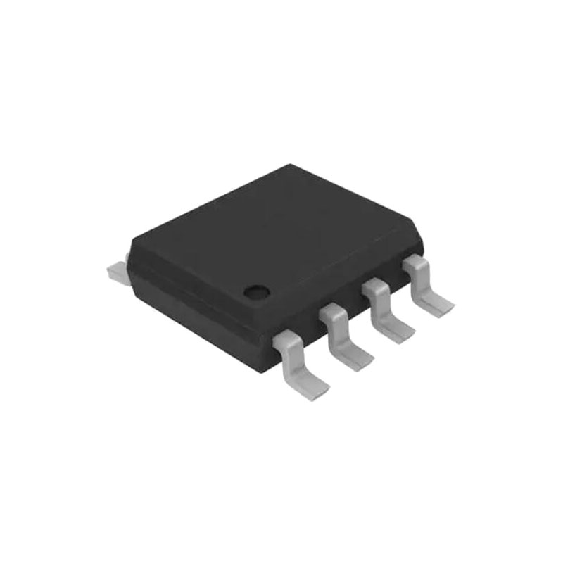
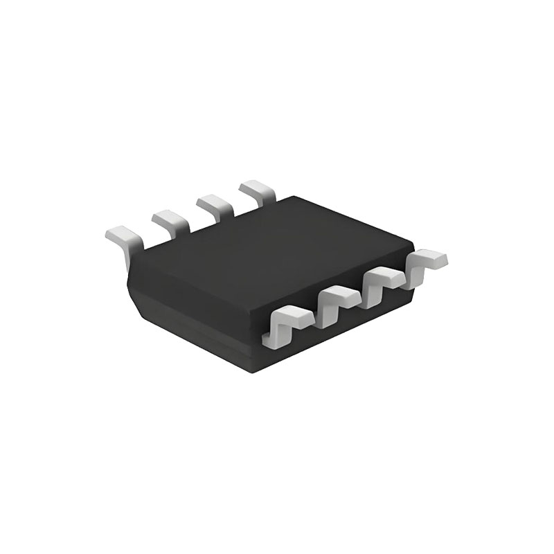
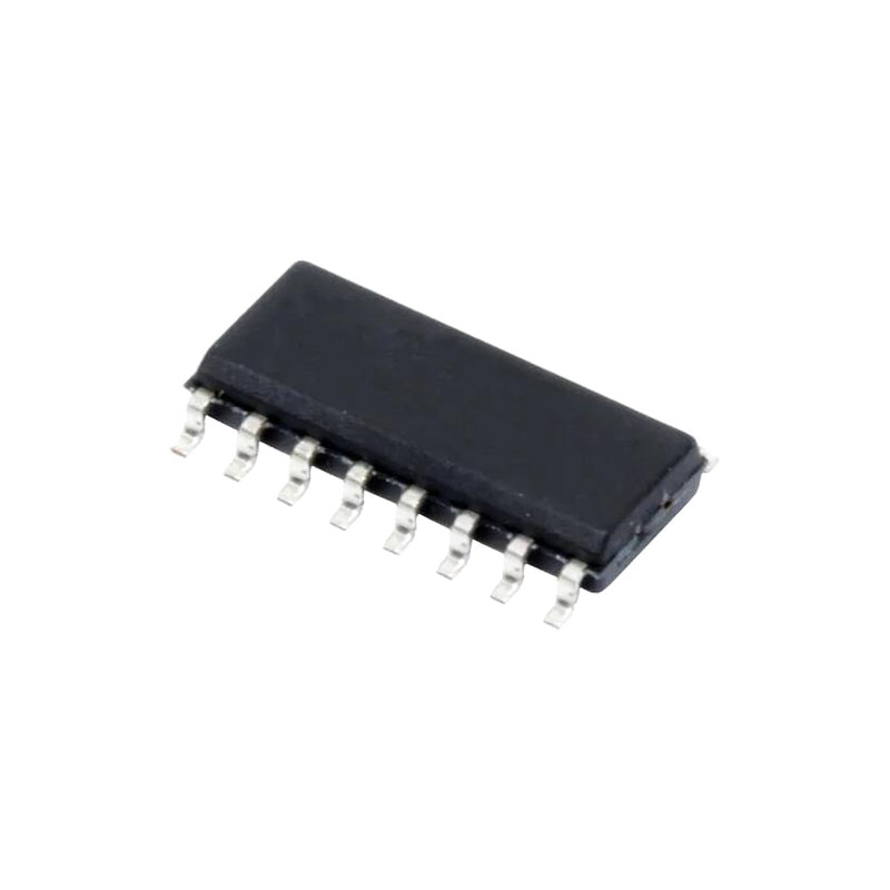
• SO8N (ECOPACK2)
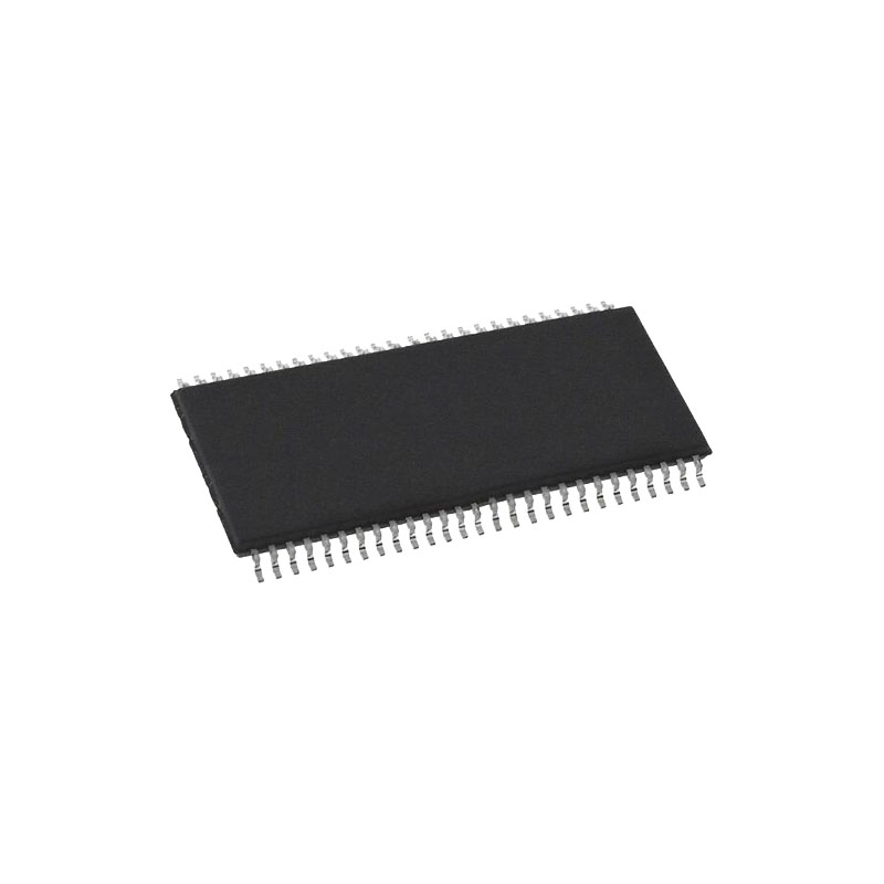
• TSSOP8 (ECOPACK2)
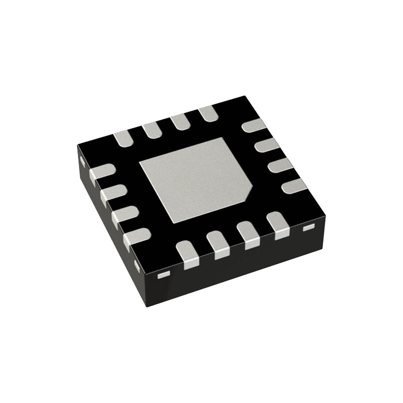
• UFDFPN8 (ECOPACK2)
• UFDFPN5 (ECOPACK2)
SIGNAL DESCRIPTION
Serial clock (SCL)
The signal applied on the SCL input is used to strobe the data available on SDA(in) and to output the data on SDA(out).
Serial data (SDA)
SDA is an input/output used to transfer data in or data out of the device. SDA(out) is an open drain output that may be wired-AND with other open drain or open collector signals on the bus. A pull-up resistor must be connected from serial data (SDA) to VCC.
Operating supply voltage (VCC)
Prior to selecting the memory and issuing instructions to it, a valid and stable VCC voltage within the specified [VCC(min), VCC(max)] range must be applied . In order to secure a stable DC supply voltage, it is recommended to decouple the VCC line with a suitable capacitor (usually of the order of 10 nF to 100 nF) close to the VCC/VSS package pins.
This voltage must remain stable and valid until the end of the transmission of the instruction and, for a write instruction, until the completion of the internal write cycle (tW).
Device reset
In order to prevent inadvertent write operations during power-up, a power-on-reset (POR) circuit is included.
At power-up, the device does not respond to any instruction until VCC has reached the internal reset threshold voltage. This threshold is lower than the minimum VCC operating voltage. When VCC passes over the POR threshold, the device is reset and enters the standby power mode; however, the device must not be accessed until VCC reaches a valid and stable DC voltage within the specified [VCC(min), VCC(max)] range .
In a similar way, during power-down (continuous decrease in VCC), the device must not be accessed when VCC drops below VCC(min). When VCC drops below the power-on-reset threshold voltage, the device stops responding to any instruction sent to it.
Power-down conditions
During power-down (continuous decrease in VCC), the device must be in the standby power mode (mode reached after decoding a stop condition, assuming that there is no internal write cycle in progress).
Read operations
Read operations are performed independently of the state of the write control (WC) signal.
For the read instructions, after each byte read (data out), the device waits for an acknowledgement (data in) during the 9th bit time. If the bus master does not acknowledge during this 9th time, the device terminates the data transfer and switches to its standby mode after a stop condition.

