DESCRIPCIÓN GENERAL
The ADuM160N/ADuM161N/ADuM162N/ADuM163N1 are 6-channel digital isolators based on Analog Devices, Inc., iCoupler technology. Combining high speed, complementary metal-oxide semiconductor (CMOS) and monolithic air core transformer technology, these isolation components provide outstanding performance characteristics superior to alternatives such as optocoupler devices and other integrated couplers. The maximum propagation delay is 13 ns with a pulse width distortion of less than 4.5 ns at 5 V operation. Channel to channel matching of propagation delay is tight at 4.0 ns maximum.
The ADuM160N/ADuM161N/ADuM162N/ADuM163N data channels are independent and are available in a variety of configurations with a withstand voltage rating of 3.0 kV rms (see the Ordering Guide).The devices operate with the supply voltage on either side ranging from 1.7 V to 5.5 V, providing compatibility with lower voltage systems as well as enabling voltage translation functionality across the isolation barrier.
Unlike other optocoupler alternatives, dc correctness is ensured in the absence of input logic transitions. Two different fail-safe options are available by which the outputs transition to a predetermined state when the input power supply is not applied.
CARACTERÍSTICAS
High common-mode transient immunity: 100 kV/µs
Gran resistencia al ruido radiado y conducido
Bajo retardo de propagación
– 13 ns maximum for 5 V operation
– 15 ns maximum for 1.8 V operation
Velocidad de datos máxima garantizada de 150 Mbps
Safety and regulatory approvals (pending)
– UL 1577
– VISO = 3000 V rms for 1 minute
– IEC/CSA 62368-1
– IEC/CSA 60601-1
– IEC/CSA 61010-1
– CQC GB 4943.1
– DIN EN IEC 60747-17 (VDE 0884-17)
– VIORM = 565 V peak
Bajo consumo dinámico
Traducción de nivel de 1,8 V a 5 V
Funcionamiento a alta temperatura: 125°C
Opciones de alta o baja a prueba de fallos
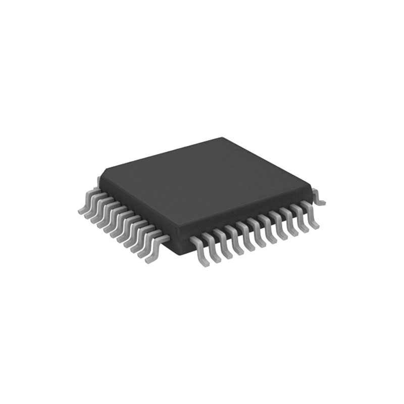
16-lead, RoHS-compliant, narrow-body SOIC package
APLICACIONES
Aislamiento multicanal de uso general
Interfaz periférica serie (SPI)/aislamiento del convertidor de datos
Aislamiento de bus de campo industrial
CARACTERÍSTICAS ELÉCTRICAS-5 V FUNCIONAMIENTO
All typical specifications are at TA = 25°C, VDD1 = VDD2 = 5 V. Minimum/maximum specifications apply over the entire recommended operation range of 4.5 V ≤ VDD1 ≤ 5.5 V, 4.5 V ≤ VDD2 ≤ 5.5 V, and −40°C ≤ TA ≤ +125°C, unless otherwise noted. Switching specifications are tested with CL = 15 pF and CMOS signal levels, unless otherwise noted. Supply currents are specified with 50% duty cycle signals.
ESPECIFICACIONES
1、150 Mbps is the highest data rate that can be guaranteed, although higher data rates are possible.
2、IOx is the Channel x output current, where x = A, B, C, D, E, or F.
3、VIxH is the input side logic high.
4、VIxL is the input side logic low.
5、VI is the voltage input.
6、N0 refers to the ADuM160N0/ADuM161N0/ADuM162N0/ADuM163N0 models. N1 refers to the ADuM160N1/ADuM161N1/ADuM162N1/ADuM163N1 models. See the Ordering Guide section.
7、|CMH| is the maximum common-mode voltage slew rate that can be sustained while maintaining the voltage output (VO) > 0.8 VDDx. |CML| is the maximum common-mode voltage slew rate that can be sustained while maintaining VO > 0.8 V. The common-mode voltage slew rates apply to both rising and falling common-mode voltage edges.
VALORES MÁXIMOS ABSOLUTOS
Las tensiones iguales o superiores a las indicadas en Valores máximos absolutos pueden provocar daños permanentes en el producto. Se trata únicamente de una clasificación de tensión; no se implica el funcionamiento funcional del producto en estas condiciones ni en ninguna otra por encima de las indicadas en la sección de funcionamiento de esta especificación. El funcionamiento durante periodos prolongados por encima de las condiciones de funcionamiento máximas puede afectar a la fiabilidad del producto.
TEORÍA DE FUNCIONAMIENTO
The ADuM160N/ADuM161N/ADuM162N/ADuM163N use a high frequency carrier to transmit data across the isolation barrier using iCoupler chip scale transformer coils separated by layers of polyimide isolation. Internal regulators and input/output design techniques allow logic and supply voltages over a wide range from 1.7 V to 5.5 V, offering voltage translation of 1.8 V, 2.5 V, 3.3 V, and 5 V logic. The architecture is designed for high common-mode transient immunity and high immunity to electrical noise and magnetic interference. Radiated emissions are minimized with a spread spectrum OOK carrier and other techniques.