DESCRIPCIÓN
The LT8645S-2 synchronous step-down regulator features Silent Switcher architecture designed to minimize EMI emissions while delivering high efficiency at high switching frequencies. This performance makes the LT8645S-2 ideal for noise sensitive applications and environments.
The fast, clean, low-overshoot switching edges enable high efficiency operation even at high switching frequencies, leading to a small overall solution size. Peak current mode control with a 40ns minimum on-time allows high step-down ratios even at high switching frequencies.
El funcionamiento en modo ráfaga permite un consumo de corriente en espera ultrabajo, el modo de salto de impulsos permite una frecuencia de conmutación completa con cargas de salida más bajas, o el funcionamiento de espectro ensanchado puede reducir aún más las emisiones EMI.
CARACTERÍSTICAS
Arquitectura del conmutador silencioso
Emisiones EMI ultrabajas
Modulación de espectro ensanchado opcional
Alta eficiencia a alta frecuencia
Hasta 95% Eficiencia a 1MHz, 12VIN a 5VOUT
Hasta 94% Eficiencia a 2MHz, 12VIN a 5VOUT
Amplio rango de tensión de entrada: 3,4 V a 65 V
Funcionamiento en modo ráfaga con corriente de reposo ultrabaja
2.5μA IQ Regulating 12VIN to 3.3VOUT
Ondulación de salida < 10mVP-P
Tiempo mínimo de encendido rápido: 40ns
Baja caída en todas las condiciones: 60mV a 1A
Ajustable y sincronizable: de 200 kHz a 2,2 MHz
Funcionamiento en modo de corriente de pico
Arranque progresivo y seguimiento de la salida
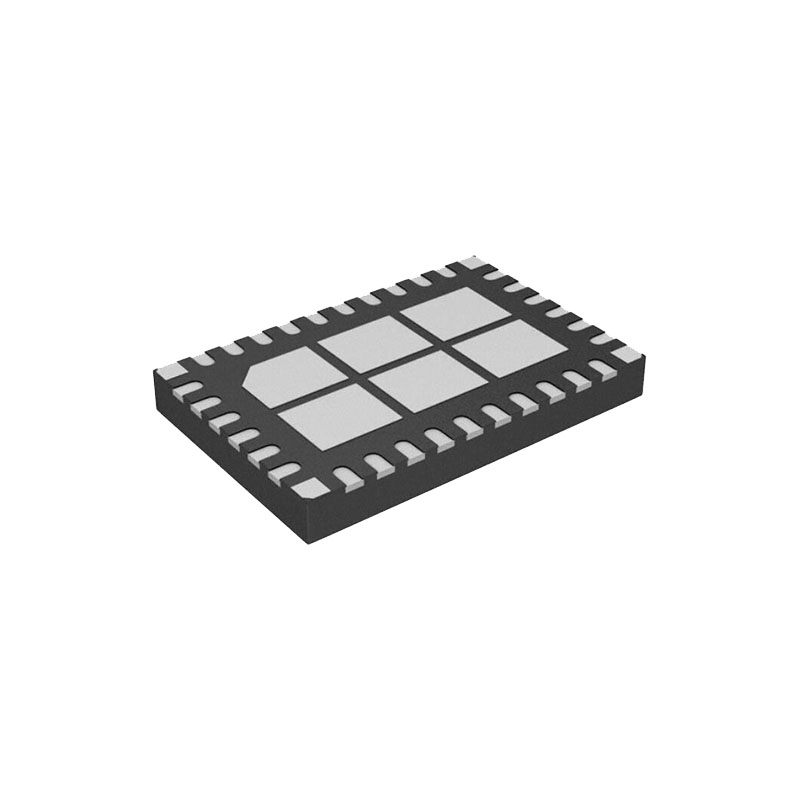
Encapsulado LQFN pequeño de 32 conductores de 6 mm × 4 mm
Cualificación AEC-Q100 para automoción
Aplicaciones
Suministros industriales y de automoción
Reductor de propósito general
Fuentes de alimentación GSM
OPERACIÓN
The LT8645S-2 is a monolithic, constant frequency, current mode step-down DC/DC converter. An oscillator, with frequency set using a resistor on the RT pin, turns on the internal top power switch at the beginning of each clock cycle. Current in the inductor then increases until the top switch current comparator trips and turns off the top power switch. The peak inductor current at which the top switch turns off is controlled by the voltage on the internal VC node. The error amplifier servos the VC node by comparing the voltage on the VFB pin with an internal 0.97V reference. When the load current increases it causes a reduction in the feedback voltage relative to the reference leading the error amplifier to raise the VC voltage until the average inductor current matches the new load current. When the top power switch turns off, the synchronous power switch turns on until the next clock cycle begins or inductor current falls to zero. If overload conditions result in more than 11A flowing through the bottom switch, the next clock cycle will be delayed until switch current returns to a safe level.
If the EN/UV pin is low, the LT8645S-2 is shut down and draws approximately 1μA from the input. When the EN/UV pin is above 1.01V, the switching regulator will become active.
To optimize efficiency at light loads, the LT8645S-2 operates in Burst Mode operation in light load situations. Between bursts, all circuitry associated with controlling the output switch is shut down, reducing the input supply current to 1.7μA. In a typical application, 2.5μA will be consumed from the input supply when regulating with no load. The SYNC/MODE pin is tied low to use Burst Mode operation and can be floated to use pulse-skipping mode. If a clock is applied to the SYNC/MODE pin, the part will synchronize to an external clock frequency and operate in pulse-skipping mode. While in pulse-skipping mode the oscillator operates continuously and positive SW transitions are aligned to the clock. During light loads, switch pulses are skipped to regulate the output and the quiescent current will be several hundred μA.
To improve EMI, the LT8645S-2 can operate in spread spectrum mode. This feature varies the clock with a triangular frequency modulation of +20%. For example, if the LT8645S-2’s frequency is programmed to switch at 2MHz, spread spectrum mode will modulate the oscillator between 2MHz and 2.4MHz. The SYNC/MODE pin should be tied high to INTVCC (~3.4V) or an external supply of 3V to 4V to enable spread spectrum modulation with pulse-skipping mode.
To improve efficiency across all loads, supply current to internal circuitry can be sourced from the BIAS pin when biased at 3.3V or above. Else, the internal circuitry will draw current from VIN. The BIAS pin should be connected to VOUT if the LT8645S-2 output is programmed at 3.3V to 25V.
Los comparadores que monitorizan la tensión de la patilla FB pondrán la patilla PG a nivel bajo si la tensión de salida varía más de ±8% (típico) del punto de consigna, o si se produce un fallo.
The oscillator reduces the LT8645S-2’s operating frequency when the voltage at the FB pin is low. This frequency foldback helps to control the inductor current when the output voltage is lower than the programmed value which occurs during start-up or overcurrent conditions. When a clock is applied to the SYNC/MODE pin, the SYNC/MODE pin is floated, or held DC high, the frequency foldback is disabled and the switching frequency will slow down only during overcurrent conditions.