DESCRIPTION GÉNÉRALE
The AD3542R is a low drift, dual channel, ultra-fast, 12-/16-bit accuracy, voltage output digital-to-analog converter (DAC) that can be configured in multiple voltage span ranges. The AD3542R operates with a fixed 2.5 V reference.
Chaque CNA incorpore trois résistances de rétroaction compensant la dérive pour l'amplificateur de transimpédance interne (TIA) qui met à l'échelle la tension de sortie. Le dispositif dispose de cinq plages de tension de sortie préconfigurées : 0 V à 2,5 V, 0 V à 5 V, 0 V à 10 V, -5 V à +5 V, et -2,5 V à +7,5 V.
The AD3542RBCPZ16 (hereafter referred to as AD3542R-16) can operate in fast mode for maximum speed or precision mode for maximum accuracy. The AD3542RBCPZ12 (hereafter referred to as AD3542R-12) has a single operation mode.
The serial peripheral interface (SPI) can be configured in dual synchronous SPI, dual SPI and single SPI (classic SPI) mode with single date rate (SDR) or double data rate (DDR), with logical levels from 1.2 V to 1.8 V.
The AD3542R is specified over the extended industrial temperature range (–40°C to +105°C).
CARACTÉRISTIQUES
Résolution 12/16 bits
16 MUPS taux de canal unique en mode rapide
11 MUPS débit de canal unique en mode précision
78 ns temps de stabilisation du petit signal pour une précision de 0,1%
100 ns de temps de stabilisation du grand signal pour une précision de 0,1%
Problème infime : <50 pV×s
Très faible latence : 5 ns
THD: −105 dB at 1 kHz for AD3542R-16 and −95 dB at 1 kHz for AD3542R-12
5 plages de tension de sortie sélectionnables
Compatible avec les niveaux logiques 1,2 V et 1,8 V
Modes SPI simple (classique) et double
Détecteurs d'erreurs multiples, dans les domaines analogique et numérique
Référence de tension interne de 2,5 V, 10 ppm/°C maximum TC
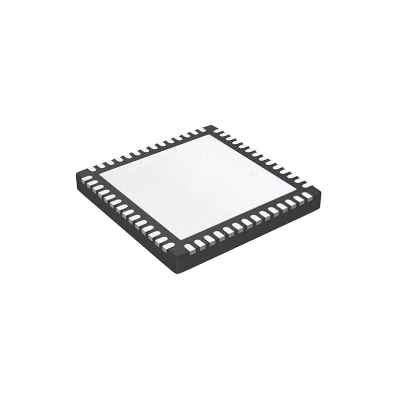
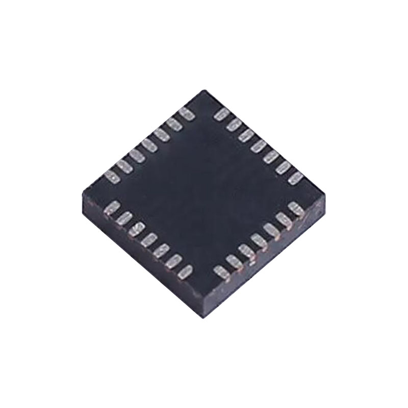
Petit boîtier : 4 mm × 4 mm LFCSP
CANDIDATURES
L'instrumentation
Le matériel dans la boucle
Équipement de contrôle des processus
Dispositifs médicaux
Équipement d'essai automatisé
Système d'acquisition de données
Sources de tension programmables
Communications optiques
THÉORIE DU FONCTIONNEMENT
Mode streaming
When the SINGLE_INSTRUCTION bit in the INTERFACE_CONFIG_ B register is set to 0, single instruction mode is disabled and streaming mode is enabled. In streaming mode, multiple registers with adjacent addresses can be accessed with a single instruction phase and data phase, allowing efficient access of contiguous regions of memory (for example, during initial device configuration). The AD3542R is configured in streaming mode by default.
En mode streaming, chaque trame SPI se compose d'une seule phase d'instruction et la phase de données suivante contient des données pour plusieurs registres avec des adresses adjacentes. Une adresse de registre de départ est spécifiée par l'hôte numérique dans la phase d'instruction, et cette adresse est automatiquement incrémentée ou décrémentée (en fonction du réglage de la direction de l'adresse) après chaque accès à un octet de données. La phase de données peut donc être longue de plusieurs octets, et chaque octet consécutif de données lues ou écrites correspond à l'adresse de registre immédiatement supérieure ou inférieure (pour une direction d'adresse ascendante ou descendante, respectivement).
Lors de l'écriture ou de la lecture d'un registre multioctet en mode continu avec adresse ascendante, l'utilisateur doit adresser l'octet le moins significatif du registre dans la phase d'instruction. La phase de données commence à transférer les données de l'octet le moins significatif en première position.
Lors de l'écriture ou de la lecture d'un registre multioctet en mode continu avec l'adresse descendante, l'utilisateur doit commencer à adresser l'octet le plus significatif du registre dans la phase d'instruction. La phase de données commence à transférer l'octet le plus significatif en première position.
INFORMATIONS SUR LES APPLICATIONS
POWER SUPPLY RECOMMENDATIONS
The AD3542R does not have any restriction for power supply sequencing. The chip incorporates a power monitor for AVDD and DVDD that releases the internal reset when both rails are within specification. Nevertheless, the recommended sequence to turn on the supply rails is GND, AVDD, DVDD, VLOGIC because it minimizes the power-up glitch. PVDD and PVSS are independent of the three previous supplies and can be switched on at any time. A small glitch (<100 mV) appears when PVDD reaches 2 V.
It is recommended to connect AGND and DGND together and have a single solid ground plane.
AVDD has a constant power consumption that is independent of the update rate. The main caution for this rail is ensuring that noise level is low in the high frequencies, where AC PSRR is lower.
DVDD has a variable power consumption that depends on the update rate and the SPI bus mode. Dynamic current has fast variations that cause the rail to be noisy. If DVDD is derived from AVDD, a filter is recommended in addition to the LDO to completely remove the effect on the DAC output.
VLOGIC has very low current demand that depends on the SPI bus mode and clock rate. Power consumption is maximum in readout operations in dual SPI mode.