DESCRIPTION GÉNÉRALE
L'AD3541R est un convertisseur numérique-analogique (DAC) à faible dérive, monocanal, ultra-rapide, d'une précision de 12/16 bits, à sortie en tension, qui peut être configuré dans plusieurs plages de tension. L'AD3541R fonctionne avec une référence fixe de 2.5V.
Chaque CNA incorpore trois résistances de rétroaction compensant la dérive pour l'amplificateur de transimpédance interne (TIA) qui met à l'échelle la tension de sortie. Le dispositif dispose de cinq plages de tension de sortie préconfigurées : 0 V à 2,5 V, 0 V à 5 V, 0 V à 10 V, -5 V à +5 V, et -2,5 V à +7,5 V.
L'AD3541RBCPZ16 (ci-après dénommé AD3541R-16) peut fonctionner en mode rapide pour une vitesse maximale ou en mode précision pour une exactitude maximale. L'AD3541RBCPZ12 (ci-après dénommé AD3541R-12) a un seul mode de fonctionnement.
L'interface périphérique série (SPI) peut être configurée en mode double SPI et simple SPI (SPI classique) avec un débit de données unique (SDR) ou double (DDR), avec des niveaux logiques de 1,2 V à 1,8 V.
L'AD3541R est spécifié sur la plage de température industrielle étendue (-40°C à +105°C).
CARACTÉRISTIQUES
Résolution 12/16 bits
16 MUPS taux de canal unique en mode rapide
11 MUPS débit de canal unique en mode précision
78 ns temps de stabilisation du petit signal pour une précision de 0,1%
100 ns de temps de stabilisation du grand signal pour une précision de 0,1%
Problème infime : <50 pV×s
Très faible latence : 5 ns
THD : -105 dB à 1 kHz pour AD3541R-16 et -95 dB à 1 kHz pour AD3541R-12
5 plages de tension de sortie sélectionnables
Compatible avec les niveaux logiques 1,2 V et 1,8 V
Modes SPI simple (classique) et double
Détecteurs d'erreurs multiples, dans les domaines analogique et numérique
Référence de tension interne de 2,5 V, 10 ppm/°C maximum TC
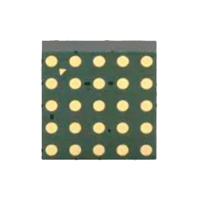
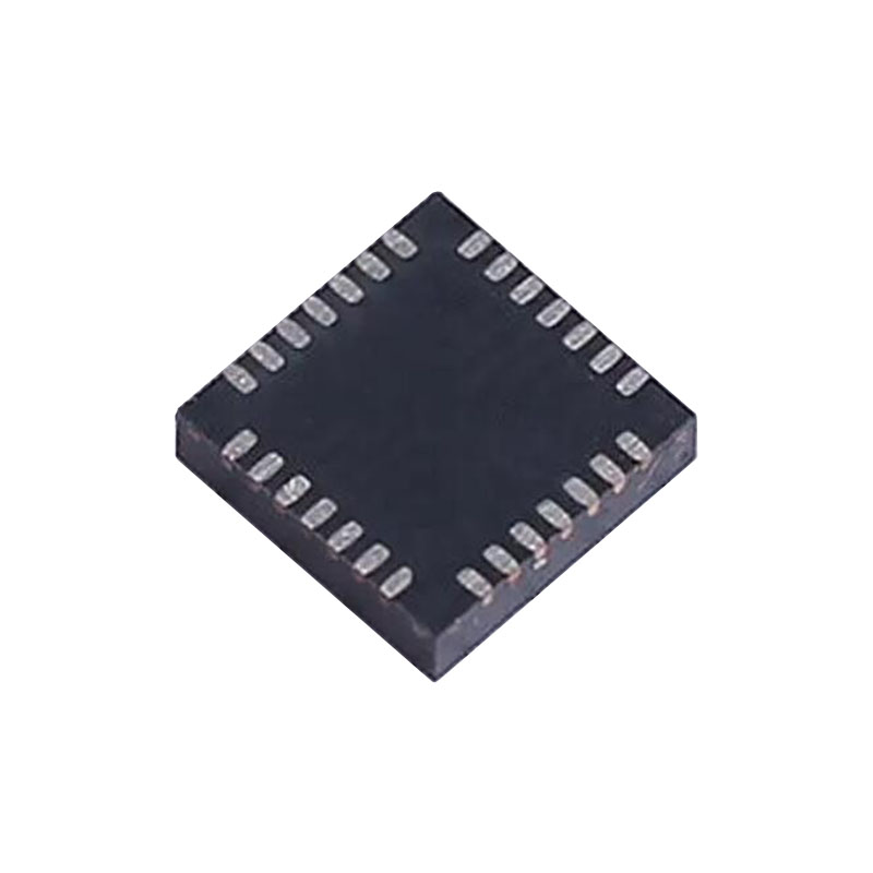
Petit boîtier : 4 mm × 4 mm LFCSP
CANDIDATURES
L'instrumentation
Le matériel dans la boucle
Équipement de contrôle des processus
Dispositifs médicaux
Équipement d'essai automatisé
Système d'acquisition de données
Sources de tension programmables
Communications optiques
THÉORIE DU FONCTIONNEMENT
Mode streaming
Lorsque le bit SINGLE_INSTRUCTION du registre INTERFACE_CONFIG_ B est mis à 0, le mode d'instruction unique est désactivé et le mode streaming est activé. En mode streaming, plusieurs registres avec des adresses adjacentes peuvent être accédés avec une seule phase d'instruction et une seule phase de données, ce qui permet un accès efficace à des régions contiguës de la mémoire (par exemple, lors de la configuration initiale du dispositif). L'AD3541R est configuré en mode streaming par défaut.
En mode streaming, chaque trame SPI se compose d'une seule phase d'instruction et la phase de données suivante contient des données pour plusieurs registres avec des adresses adjacentes. Une adresse de registre de départ est spécifiée par l'hôte numérique dans la phase d'instruction, et cette adresse est automatiquement incrémentée ou décrémentée (en fonction du réglage de la direction de l'adresse) après chaque accès à un octet de données. La phase de données peut donc être longue de plusieurs octets, et chaque octet consécutif de données lues ou écrites correspond à l'adresse de registre immédiatement supérieure ou inférieure (pour une direction d'adresse ascendante ou descendante, respectivement).
Lors de l'écriture ou de la lecture d'un registre multioctet en mode continu avec adresse ascendante, l'utilisateur doit adresser l'octet le moins significatif du registre dans la phase d'instruction. La phase de données commence à transférer les données de l'octet le moins significatif en première position.
Lors de l'écriture ou de la lecture d'un registre multioctet en mode continu avec l'adresse descendante, l'utilisateur doit commencer à adresser l'octet le plus significatif du registre dans la phase d'instruction. La phase de données commence à transférer l'octet le plus significatif en première position.
Le registre STREAM_MODE peut être utilisé pour spécifier une plage de registres consécutifs à parcourir en boucle dans la phase de données. Le bouclage permet à l'hôte numérique de lire ou d'écrire de manière répétée dans un ensemble de registres (par exemple, le registre CHx_DAC_16B à l'adresse 0x29 jusqu'à l'adresse 0x2C) de la manière la plus efficace possible. Lors de l'accès aux adresses de registre après l'adresse 0x29 incluse, la direction de l'adresse doit toujours être définie comme descendante.