概要
The AD3542R is a low drift, dual channel, ultra-fast, 12-/16-bit accuracy, voltage output digital-to-analog converter (DAC) that can be configured in multiple voltage span ranges. The AD3542R operates with a fixed 2.5 V reference.
各DACは、出力電圧をスケーリングする内部トランスインピーダンス・アンプ(TIA)用に、3つのドリフト補償フィードバック抵抗を内蔵しています。このデバイスには、あらかじめ設定された5つの出力電圧範囲があります:0 V~2.5 V、0 V~5 V、0 V~10 V、-5 V~+5 V、および-2.5 V~+7.5 Vです。
The AD3542RBCPZ16 (hereafter referred to as AD3542R-16) can operate in fast mode for maximum speed or precision mode for maximum accuracy. The AD3542RBCPZ12 (hereafter referred to as AD3542R-12) has a single operation mode.
The serial peripheral interface (SPI) can be configured in dual synchronous SPI, dual SPI and single SPI (classic SPI) mode with single date rate (SDR) or double data rate (DDR), with logical levels from 1.2 V to 1.8 V.
The AD3542R is specified over the extended industrial temperature range (–40°C to +105°C).
特徴
12/16ビット解像度
高速モードで16 MUPSシングル・チャンネル・レート
11 MUPSシングル・チャンネル・レート(プレシジョン・モード時
0.1% 精度までの小信号整定時間 78 ns
0.1% 精度までの大信号セトリング時間 100 ns
超小型の不具合:<50pV×s未満
超低レイテンシ:5 ns
THD: −105 dB at 1 kHz for AD3542R-16 and −95 dB at 1 kHz for AD3542R-12
選択可能な5つの出力電圧範囲
1.2Vおよび1.8Vロジックレベル対応
シングル(クラシック)およびデュアルSPIモード
アナログとデジタルの両方で複数のエラー検出器
2.5 V 内部電圧基準、最大 TC 10 ppm/°C
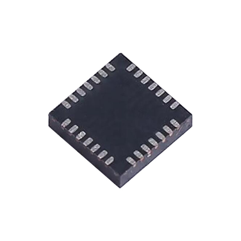
小型パッケージ:4mm×4mm LFCSP
アプリケーション
計装
ループ内のハードウェア
プロセス制御機器
医療機器
自動試験装置
データ収集システム
プログラマブル電圧源
光通信
動作理論
ストリーミング・モード
When the SINGLE_INSTRUCTION bit in the INTERFACE_CONFIG_ B register is set to 0, single instruction mode is disabled and streaming mode is enabled. In streaming mode, multiple registers with adjacent addresses can be accessed with a single instruction phase and data phase, allowing efficient access of contiguous regions of memory (for example, during initial device configuration). The AD3542R is configured in streaming mode by default.
ストリーミング・モードの場合、各SPIフレームは1つの命令フェーズで構成され、次のデータ・フェーズには隣接するアドレスを持つ複数のレジスタのデータが含まれます。開始レジスタ・アドレスは命令フェーズでデジタル・ホストによって指定され、このアドレスはデータの各バイトがアクセスされるたびに(アドレス方向の設定に基づいて)自動的にインクリメントまたはデクリメントされます。したがって、データ・フェーズは複数バイト長にすることができ、読み出しデータまたは書き込みデータの各連続バイトは、次の上位または下位レジスタ・アドレスに対応します(それぞれ、アドレス方向が昇順および降順の場合)。
アドレス昇順のストリーミング・モードでマルチバイト・レジスタから書き込みまたは読み出しを行う場合、ユーザーは命令フェーズでレジスタの最下位バイトをアドレス指定する必要があります。データ・フェーズでは、最下位バイトの先頭からデータの転送が開始されます。
ストリーミング・モードでマルチバイト・レジスタをアドレス降順で書き込んだり読み出したりする場合、ユーザは命令フェーズでレジスタの最上位バイトからアドレスを指定しなければなりません。データ・フェーズでは、最上位バイトから転送が開始されます。
アプリケーション情報
POWER SUPPLY RECOMMENDATIONS
The AD3542R does not have any restriction for power supply sequencing. The chip incorporates a power monitor for AVDD and DVDD that releases the internal reset when both rails are within specification. Nevertheless, the recommended sequence to turn on the supply rails is GND, AVDD, DVDD, VLOGIC because it minimizes the power-up glitch. PVDD and PVSS are independent of the three previous supplies and can be switched on at any time. A small glitch (<100 mV) appears when PVDD reaches 2 V.
It is recommended to connect AGND and DGND together and have a single solid ground plane.
AVDD has a constant power consumption that is independent of the update rate. The main caution for this rail is ensuring that noise level is low in the high frequencies, where AC PSRR is lower.
DVDD has a variable power consumption that depends on the update rate and the SPI bus mode. Dynamic current has fast variations that cause the rail to be noisy. If DVDD is derived from AVDD, a filter is recommended in addition to the LDO to completely remove the effect on the DAC output.
VLOGIC has very low current demand that depends on the SPI bus mode and clock rate. Power consumption is maximum in readout operations in dual SPI mode.