概要
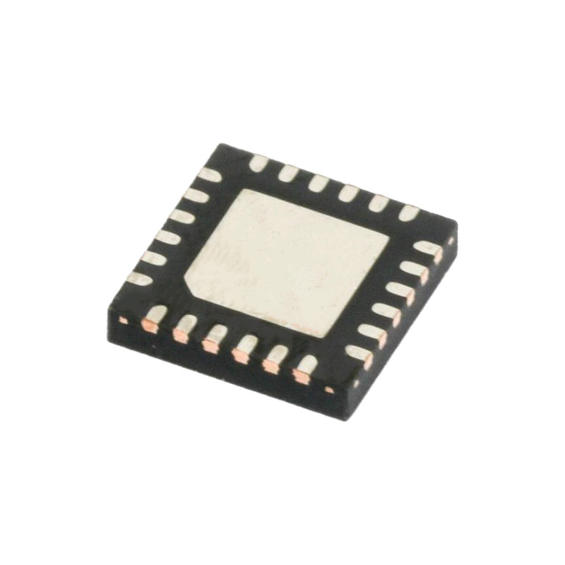
The AD3551R is a low drift, single channel, ultra-fast, 16-bit accuracy, current output digital-to-analog converter (DAC) that can be configured in multiple voltage span ranges. The AD3551R operates with a fixed 2.5 V reference.
各DACは、出力電圧をスケーリングする外部トランスインピーダンス・アンプ(TIA)に必要な3つのドリフト補償フィードバック抵抗を内蔵しています。オフセットとゲインのスケーリング・レジスタにより、0 V~2.5 V、0 V~5 V、0 V~10 V、-5 V~+5 V、-10 V~+10 Vなどの複数の出力スパン・レンジや、フル16ビット分解能のカスタム中間レンジを生成できます。
DACは、最高速度の高速モードまたは最高精度の精密モードで動作することができる。
The serial peripheral interface (SPI) can be configured in quad SPI mode, dual SPI mode, and single SPI (classic SPI) mode with single date rate (SDR) or double data rate (DDR), with logical levels from 1.2 V to 1.8 V.
The AD3551R is specified over the extended industrial temperature range (–40°C to +105°C).
特徴
16ビット分解能
高速モードで33 MUPSレート
22MUPSレート(高精度モード
0.1% 精度までの小信号整定時間 65 ns
0.1% 精度までの大信号セトリング時間 100 ns
超小型グリッチ:< 50 pV×s
超低遅延:5 ns
THD:-105 dB(1 kHz時
高度に設定可能な出力電圧スパンとオフセット
1.2Vおよび1.8Vロジックレベル対応
シングル(クラシック)、デュアル、クアッドSPIモード
アナログとデジタルの両方で複数のエラー検出器
2.5 V内部電圧リファレンス、最大温度係数10 ppm/°C
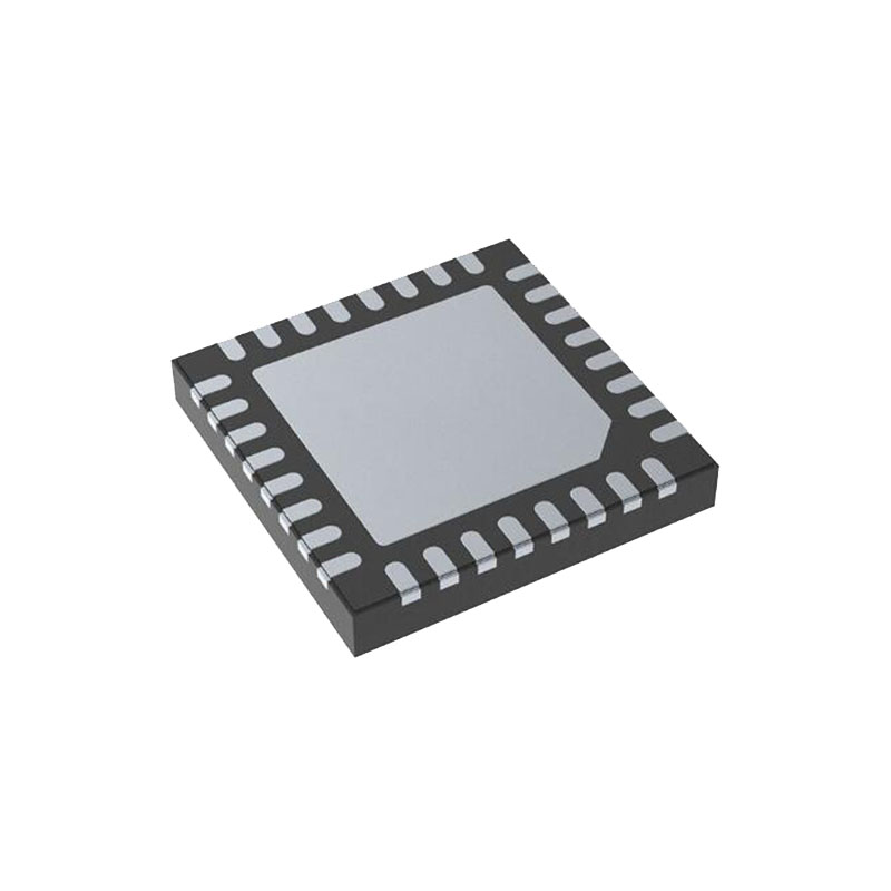
5 mm × 5 mm LFCSP
アプリケーション
計装
ループ内のハードウェア
プロセス制御機器
医療機器
自動試験装置
データ収集システム
プログラマブル電圧源
光通信
アプリケーション情報
POWER SUPPLY RECOMMENDATIONS
The AD3551R does not have any restriction for power supply sequencing. The chip incorporates a power monitor for AVDD and DVDD that releases the internal reset when both rails are within specification. Nevertheless, the recommended sequence to turn on the supply rails is GND, AVDD, DVDD, VLOGIC because it minimizes the power-up glitch.
It is recommended to connect AGND and DGND together and have a single solid ground plane. The exposed pad under the chip must also be connected to the ground plane.
AVDD has a constant power consumption that is independent of the update rate. The main caution for this rail is ensuring that noise level is low in the high frequencies, where AC PSRR is lower.
DVDD has a variable power consumption that depends on the update rate and the SPI bus mode. Dynamic current has fast variations that cause the rail to be noisy. If DVDD is derived from AVDD, a filter is recommended in addition to the LDO to completely remove the effect on the DAC output.
VLOGIC has very low current demand that depends on the SPI bus mode and clock rate. Power consumption is maximum in readout operations in quad SPI mode.
The decoupling capacitors on PCAPx, NCAPx, VCMx, and CVREF can be adjusted to achieve the desired trade-off between noise corner frequency and power-up glitch amplitude.
Use capacitors with NP0 dielectric for the NCAPx and PCAPx feedback capacitors and any other capacitors on the path of the output voltage to avoid the derating caused by low frequency voltage variations. The decoupling capacitors for the supply rails, VCM and CVREF, can use materials with high dielectric constant because the voltage on these lines is constant.
レイアウトガイドライン
The following list is a few recommendations to observe to obtain the best performance:
Keep IOUT lines as short and thin as possible. This signal is responsible for the slewing of the amplifier to the final value. Therefore, the parasitic capacitance on this line increases the settling time. Use a feedback capacitor with a small footprint to minimize parasitic capacitance to the ground plane.
Keep the IOUT line away from repetitive signals, such as clocks and analog signals with high voltage excursion, because this is a high impedance line that can easily pick up electromagnetic interference.
Connect the exposed pad of the AD3551R to the ground plane with several vias to minimize thermal drift. Note that the chip can dissipate up to 150 mW.
Keep switching regulators and fast dV/dt signals away from the feedback loops of the DAC. Any μA induced on these lines becomes a mV at the output of the DAC.
Do not overlap analog and digital signals. If a crossing cannot be avoided, it must be done at 45° or 90°.
Route digital lines using traces with a constant characteristic impedance to avoid signal integrity problems that result in timing violations in DDR mode and crosstalk between signals. The traces must have a continuous ground plane underneath. When changing layers, ensure that the destination layer is referred to another ground plane and the traces have the same characteristic impedance. Place a via connecting both ground planes near the via of the digital line. If the destination layer is referred to a power plane, it must be continuous along the path of the line and a decoupling capacitor between power and ground must be placed close to the via of the digital line.

