DESCRIPTION
The LT8640S/LT8643S/LT8640SA/LT8643SA synchronous step-down regulator features second generation Silent Switcher architecture designed to minimize EMI emissions while delivering high efficiency at high switching frequencies. This includes the integration of bypass capacitors to optimize all the fast current loops inside and make it easy to achieve advertised EMI performance by reducing layout sensitivity. This performance makes the LT8640S/LT8643S/LT8640SA/LT8643SA ideal for noisesensitive applications and environments. Peak current mode control with a 30ns minimum on-time allows high step-down ratios even at high switching frequencies. The LT8643S/LT8643SA has external compensation to enable current sharing and fast transient response at high switching frequencies. Burst Mode operation enables ultralow standby current consumption, forced continuous mode can control frequency harmonics across the entire output load range, or spread spectrum operation can further reduce EMI emissions.
FEATURES
Silent Switcher 2 Architecture
Ultralow EMI Emissions on Any PCB
Eliminates PCB Layout Sensitivity
Internal Bypass Capacitors Reduce Radiated EMI
Optional Spread Spectrum Modulation
High Efficiency at High Frequency
Up to 96% Efficiency at 1MHz, 12VIN to 5VOUT
Up to 95% Efficiency at 2MHz, 12VIN to 5VOUT
Wide Input Voltage Range: 3.4V to 42V
Output Voltage Range: 0.97V to 10V(LT8640S/LT8643S); 0.97V to (VIN – 0.5V) (LT8640SA/LT8643SA)
6A Maximum Continuous, 7A Peak Output
Ultralow Quiescent Current Burst Mode® Operation
2.5μA IQ Regulating 12VIN to 3.3VOUT (LT8640S/LT8640SA)
Output Ripple < 10mVP-P
External Compensation: Fast Transient Response and Current Sharing (LT8643S/LT8643SA)
Robust High VOUT Operation (LT8640SA/LT8643SA)
Safely Tolerates High Reverse Current
Fast Minimum Switch On-Time: 30ns
Low Dropout Under All Conditions: 100mV at 1A
Forced Continuous Mode
Adjustable and Synchronizable: 200kHz to 3MHz
Output Soft-Start and Tracking
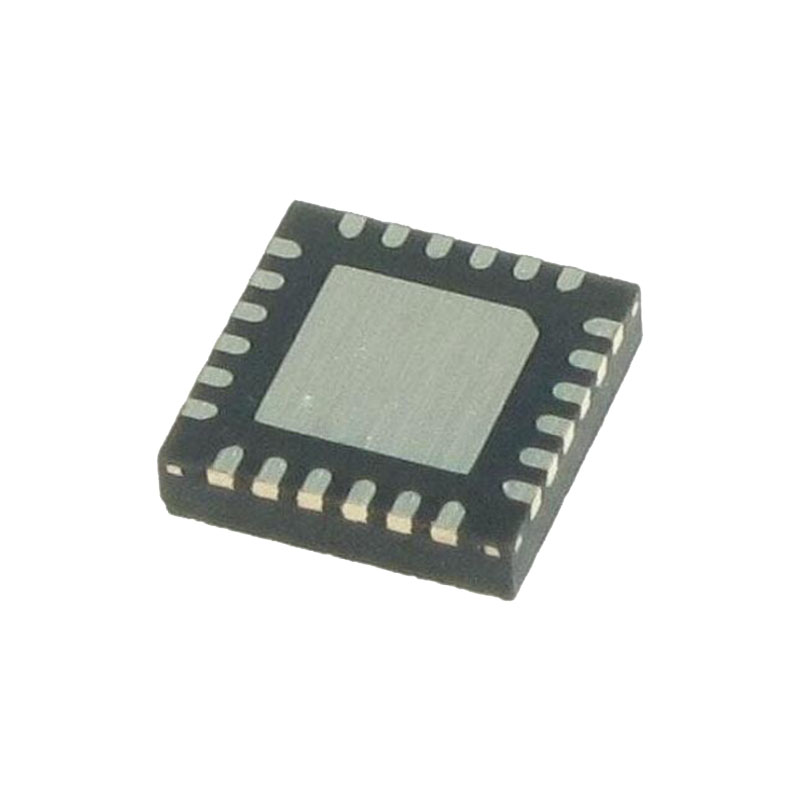
Small 24-Lead 4mm × 4mm LQFN Package
AEC-Q100 Qualified for Automotive
Applications
Automotive and Industrial Supplies
OPERATION
The LT8640S/LT8643S/LT8640SA/LT8643SA is a monolithic, constant frequency, current mode step-down DC/DC converter. An oscillator, with frequency set using a resistor on the RT pin, turns on the internal top power switch at the beginning of each clock cycle. Current in the inductor then increases until the top switch current comparator trips and turns off the top power switch. The peak inductor current at which the top switch turns off is controlled by the voltage on the internal VC node. The error amplifier servos the VC node by comparing the voltage on the VFB pin with an internal 0.97V reference. When the load current increases it causes a reduction in the feedback voltage relative to the reference leading the error amplifier to raise the VC voltage until the average inductor current matches the new load current. When the top power switch turns off, the synchronous power switch turns on until the next clock cycle begins or inductor current falls to zero. If overload conditions result in more than 10A flowing through the bottom switch, the next clock cycle will be delayed until switch current returns to a safe level.
The “S” in LT8640S/LT8643S/LT8640SA/LT8643SA refers to the second generation silent switcher technology. This technology allows fast switching edges for high efficiency at high switching frequencies, while simultaneously achieving good EMI performance. This includes the integration of ceramic capacitors into the package for VIN, BST, and INTVCC (see Block Diagram). These caps keep all the fast AC current loops small, which improves EMI performance.
If the EN/UV pin is low, the LT8640S/LT8643S/LT8640SA/ LT8643SA is shut down and draws 1μA from the input. When the EN/UV pin is above 1V, the switching regulator will become active.
To optimize efficiency at light loads, the LT8640S/LT8643S/ LT8640SA/LT8643SA operates in Burst Mode operation in light load situations. Between bursts, all circuitry associated with controlling the output switch is shut down, reducing the input supply current to 1.7μA (LT8640S/ LT8640SA) or 230μA (LT8643S/LT8643SA with BIAS = 0). In a typical application, 2.5μA (LT8640S/LT8640SA) or 120μA (LT8643S/LT8643SA with BIAS = 5VOUT) will be consumed from the input supply when regulating with no load. The SYNC/MODE pin is tied low to use Burst Mode operation and can be floated to use forced continuous mode (FCM). If a clock is applied to the SYNC/MODE pin, the part will synchronize to an external clock frequency and operate in FCM.