Описание
The TLV3201 and TLV3202 are single- and dual-channel comparators that offer the ultimate combination of high speed (40ns) and low-power consumption (40µA), all in extremely small packages with features such as rail-to-rail inputs, low offset voltage (1mV ), and large output drive current. The devices are also very easy to implement in a wide variety of applications where response time is critical.
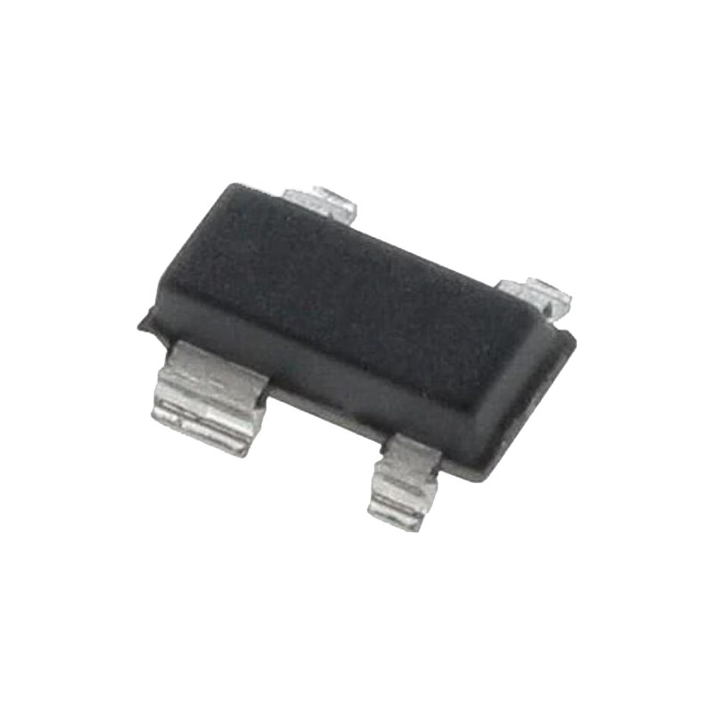
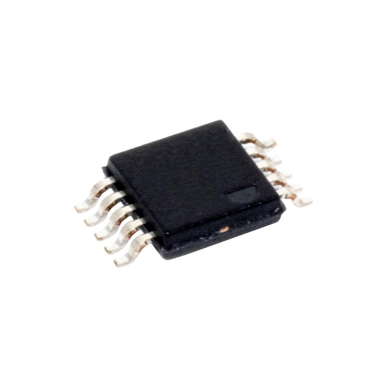
The TLV320x family is available in single (TLV3201) and dual (TLV3202) channel versions, both with push-pull outputs. The TLV3201 is available in 5-pin SOT-23 and 5-pin SC70 packages. The TLV3202 is available in 8-pin SOIC and 8-pin VSSOP packages. All devices are specified for operation across the expanded industrial temperature range of –40°C to 125°C.
Характеристики
• Low Propagation Delay: 40ns
• Low Quiescent Current: 40µA per Channel
• Input Common-Mode Range Extends 200mV Beyond Either Rail
• Low Input Offset Voltage: 1mV
• Push-Pull Outputs
• Supply Range: 2.7V to 5.5V
• Industrial Temperature Range:–40°C to 125°C
• Small Packages: 5-Pin SC70, 5-Pin SOT-23, 8-Pin SOIC, 8-Pin VSSOP
Приложения
• Inspection Equipment
• Test and Measurement
• High-Speed Sampling Systems
• Telecom
• Portable Communications
More Information Description
Обзор
The TLV3201 and TLV3202 devices feature 40ns response time, and include 1.2mV of internal hysteresis for improved noise immunity with an input common-mode range that extends 0.2V beyond the power-supply rails.
Рабочее напряжение
The TLV3201 and TLV3202 comparators are specified for use on a single supply from 2.7V to 5.5V (or a dual supply from ±1.35V to ±2.75V) over a temperature range of −40°C to 125°C. The device continues to function below this range, but performance is not specified.
Input Overvoltage Protection
The device inputs are protected by electrostatic discharge (ESD) diodes that conduct if the input voltages exceed the power supplies by more than approximately 300mV . Momentary voltages greater than 300mV beyond the power supply can be tolerated if the input current is limited to 10mA. This limiting is easily accomplished with a small input resistor in series with the input to the comparator.
Функциональные режимы устройства
The device is fully functional when powered by rail-to-rail supply voltage greater than 2.7V. The device is off at any voltages below 2.7V.
Информация о заявке
The TLV3201 and TLV3202 are single- and dual-supply (respectively), push-pull comparators featuring 40ns of propagation delay on only 40µA of supply current. This combination of fast response time and minimal power consumption make the TLV3201 and TLV3202 excellent comparators for portable, battery-powered applications as well as fast-switching threshold detection such as pulse-width modulation (PWM) output monitors and zerocross detection.
Рекомендации по источникам питания
The TLV3201 and TLV3202 comparators are specified for use on a single supply from 2.7V to 5.5V (or a dual supply from ±1.35V to ±2.75V) over a temperature range of −40°C to 125°C. The device continues to function below this range, but performance is not specified. Place bypass capacitors close to the power-supply pins to reduce noise coupling in from noisy or high-impedance power supplies. For more detailed information on bypass capacitor placement,
Рекомендации по компоновке
The TLV3201 and TLV3202 are fast-switching, high-speed comparators and require high-speed layout considerations. For best results, maintain the following layout guidelines.
• Use a printed-circuit board (PCB) with a good, unbroken low-inductance ground plane.
• Place a decoupling capacitor (0.1µF ceramic, surface-mount capacitor) as close as possible to VCC.
• On the inputs and the output, keep lead lengths as short as possible to avoid unwanted parasitic feedback around the comparator. Keep inputs away from the output.
• Solder the device directly to the PCB rather than using a socket.
• For slow-moving input signals, take care to prevent parasitic feedback. A small capacitor (1000pF or less) placed between the inputs can help eliminate oscillations in the transition region. This capacitor causes some degradation to propagation delay when the impedance is low. The topside ground plane runs between the output and inputs.
• The ground pin ground trace runs under the device up to the bypass capacitor, shielding the inputs from the outputs.